Author Archives: abarua

Registers, registers & registers…

Ever since I read the microcontroller data sheet I’ve been working directly with their registers to achieve the functionality of the libraries in a much speedier manner utilizing minimal resources. This post is a cheat-sheet of the registers to save one the trouble of having to go through the entire data sheet everytime.

Registers of the ATmega328

Power play:

Register Bits Purpose
SMCR SE
SM0
SM1
SM2
Sleep Mode Control Register
SE bit must be written to 1 to enable sleep mode. SM[0:2] control the sleep mode (Idle, Power-down, Power-save etc.)
 MCUCR BODS
BODSE
Enables turning of BOD during sleep mode
 PRR PRTWI
PRTIM2
PRTIM1
PRTIM0
PRSPI
PRUSART0
PRADC
Power Reduction Register
Write 1 to shut-down TWI (PRTWI). TIM2: timer/counter 2. TIM1: timer 1. TIM0: timer 0. SPI: shut-down SPI. USART0 – shut-down USART by stopping the clock. PRADC – shut-down the ADC. ADC must be disabled before shut-down.

Interrupts:
Interrupt vectors are documented here.

Register Bits Purpose
EICRA ISC00
ISC01
ISC10
ISC11
External Interrupt Control Register A
ICS0[1:0] combine to determine how level on INT0 pin is interrupted. (0x0 – low level generates request, 0x1 – logical change, 0x2 – falling edge & 0x3 – rising edge. Similarly ICS1[1:0] determines the interpretation of INT1.
EIMSK INT0
INT1
External Interrupt Mask Register
Set bit to 1 to enable interrupt on INT0 or INT1.
EIFR INTF0
INTF1
External interrupt Flag register
Is set to 1 when an interrupt request is triggered. Interrupt routine execution automatically clears this flag. So, I’ve not had any occasion to use this register.
PCICR PCIE2
PCIE1
PCIE0
Pin Change Interrupt Control Register
PCIE0: interrupt enable 0 (for PCINT[7:0])
PCIE1: interrupt enable 0 (for PCINT[14:8])
PCIE2: interrupt enable 0 (for PCINT[23:16])
PCIFR PCIF2
PCIF1
PCIF0
Pin Change Interrupt Flag Register
Bit is set when interrupt request is made. Again since the interrupt routine auto clears is I haven’t found use of this register
PCMSK2 PCINT23
PCINT22

PCINT16
Pin Change Mask Register 2
Selects whether pin change interrupt is enabled on the corresponding I/O pin
PCMSK1 PCINT14
PCINT13

PCINT8
Pin Change Mask Register 1
PCMSK0 PCINT7
PCINT6

PCINT0
Pin Change Mask Register 0

I/O Ports

Register Bits Purpose
PORTB, PORTC, PORTD PORTB7
PORTB6

PORTB0

PORTC6
PORTC5
….
PORTC0

PORTD7
PORTD6

PORTD0
PORT Data Register – set 1 to set output pin high, 0 to set low. See table with DDRx registers for all combinations of Input, Output & Input with pull-up
DDRB, DDRC, DDRD DDB7

DDB0

DDC6

DDC0

DDD7

DDD0
Port Data Direction register
PINB, PINC, PIND PINB7

PINB0

PINC6

PINC0

PIND7

PIND0
Port Input register.

Timer/Counter 0 – also used by the Arduino libraries to drive millis, micros, delay, etc.

Register Bits Purpose
TCCR0A WGM00
WGM01
COM0A0
COM0A1
COM0B0
COM0B1
COM bits control the output compare pin behaviour (OC0A and OC0B). I typically use one of 2 cases: COM0A[1:0] = 0x0 – OC0A disconnected. 0x1 – Toggle on compare match in non-PWM mode (so that the frequency of the output can be varied using compare match – OCRA). For PWM use 0x2 and 0x3. Note that in PWM the frequency cannot be influenced. It always counts from BOTTOM to TOP.
The WGM bits along with WGM02 from TCCR0B drives the waveform generation (CTC, PWM, Fast PWM etc.)
TCCR0B WGM02
CS02
CS01
CS00
WGM bit is used as described above.
The CS bits are used to stop/start the clock and also set the prescaler.
CS0[2:0] – 0x0 – clock stopped. 0x1 – no prescaling. 0x2 – prescaler = 8… clock 8 times slower. 0x3 – 64. 0x4 – 256. 0x5 – 1024.
TCNT0 Timer/Counter Register
OCCR0A Output Compare Register A – match can generate output compare interrupt or generate a waveform output on OC0A pin.
OCR0B OCR B – can generate output compare interrupt or generate waveform. Note however that frequency of waveform can only be altered by OCRA and not by OCRB. This can be deduced from the waveform generation table where the TOP of the counter can only be influenced by OCRA. Otherwise it always counts up to 0xFF. Of course the frequency can be influenced by the clock speed and prescaler but to very specific values only.
TIMSK0 TOIE0
OCIE0A
OCIE0B
Interrupt Mask Register
TOIE0: when written to 1 will enable interrupt when timer overflow occurs.
OCIE0A: when written to 1 will enable interrupt on compare match A
OCIE0B: enables interrupt on compare match B.
TIFR0 TOV0
OCF0A
OCF0B
Interrupt Flag Register
TOV0: Timer overflow flag
OCF0A – set when timer matches OCR0A.
OCF0B – set when timer matches OCR0B.
Since the flags are auto-cleared on execution of interrupt I haven’t found use for this register.

Timer/Counter 1

Register Bits Purpose
TCCR1A WGM10
WGM11
COM1A0
COM1A1
COM1B0
COM1B1
Register A similar to that of Timer 0 but with some differences.
COM bits behave similarly for pins OC1A and OC1B.
The WGM bits are combined with 2 more bits from TCCR1B – WGM12 and WGM13 – to determine the waveform.
Waveforms have a bigger range including higher resolution PWM and also the ability to influence the frequency in PWM mode.
To influence the frequency in PWM mode – use mode where TOP = ICR1; and use OCR1A to influence the duty cycle.
TCCR1B WGM12
WGM13
CS10
CS11
CS12
ICNC1
ICES1
Similar to timer 0. Don’t fully understand the purpose of IC bits yet.
TCNT1 (TCNT1H,TCNT1L) 16-bit timer counter.
OCR1A (OCR1AH, OCR1AL) 16-bit compare register A
OCR1B (OCR1BH, OCR1BL) 16-bit compare register B
ICR1 (ICR1H, ICR1L) 16-bit input capture register 1
TIMSK1 TOIE1
OCIE1A
OCIE1B
ICIE1
Interrupt mask register.
TOIE1 – overflow
OCIE1* – output compare
ICIE1 – input capture interrupt enable
TIFR1 TOV1
OCF1A
OCF1B
ICF1
Interrupt Flag Register
Look at timer 0 for details. Again, I haven’t found occasion to use this yet.

Timer/Counter 2

Register Bits Purpose
TCCR2A WGM20
WGM21
COM2A0
COM2A1
COM2B0
COM2B1
Similar to timer 0. COM ports can drive OC2A and OC2B.
WGM bits along with WGM22 drive the waveforms.
TCCR2B WGM22
CS20
CS21
CS22
Similar to timer 0. CS bits drive the clock source & prescaler.
TCNT2 Timer/Counter register.
OCR2A Output Compare Register A
OCR2B OCR B
TIMSK2 TOIE2
OCIE2A
OCIE2B
Interrupt mask register.
Overflow (TOIE2) and output compare (OCIE2*)
TIFR2 TOV2
OCF2A
OCF2B
Similar to Timer 0. I don’t use it.

SPI
Key points about SPI:

  • Try and have one master and one or more slaves. Accordingly set the MSTR flag.
  • Choose the right data mode by looking at the picture. Data mode indicates whether SCK is High or Low at rest, whether data is sampled at the rising or falling edge (and naturally setup of the data at the other edge)
  • Choose whether MSB or LSB is transmitted first when serialising.
  • Choose SCK frequency with a pre-scaler (2, 4, 8,… 128)
  • In master mode, initiate a transfer by writing to SPDR; then check until SPIF flag is set to read the result. Remember sending a byte always gets a byte back even if it’s to be discarded.
  • In slave mode, the interrupt routine can be used to detect incoming data. If data should be sent back then it should be written to SPDR beforehand.
  • The Slave Select pin is held low by the Master when communicating with the slave. This is typically done in software by writing 0, then transmitting and then writing 1. Multiple bytes can be transmitted together between taking it low and then high. Datasheets for devices provide timing information (eg. every command might need the Slave Select to go from High to Low, enforced delays etc.)
Register Bits Purpose
SPCR SPE
SPIE
DORD
MSTR
CPOL, CPHA
SPR0, SPR1
SPI Control Register
SPE: SPI enable
SPIE: SPI Interrupt Enable (when serial transfer is complete – when SPIF is set)
DORD: 1 chooses LSB. 0 chooses MSB.
MSTR: 1 chooses master. 0 chooses slave.
CPOL, CPHA – drive data mode. Look at picture and ideally use the library constants.
SPR[1:0] – clock rate selection (use with SPI2X) – use library to set.
SPSR SPIF
WCOL
SPI2X
SPI Status Register
SPIF: SPI interrupt flag. Cleared when interrupt routine is run. Or when SPSR is read with SPIF set and SPDR is accessed.
SPDR SPI Data Register
read/write register.

USART0

Register Bits Purpose

TWI

Register Bits Purpose

Analog Comparator
Compares the input values on the positive pin AIN0 and negative pin AIN1. When +ve is greater than -ve ACO is set. It can also be made to trigger an interrupt – choice of rising, falling or toggle edge of AC0. The negative voltage can be replaced by any of ADC7…0. ACME must be set and ADC should be switched off (ADEN = 0). The positive voltage can be replaced by the bandgap voltage using ACBG.

Register Bits Purpose
ACSR ACD
ACBG
ACIE
ACI
ACIS1, ACIS0
ACIC
ACO
Analog Comparator Control & Status Register
ACD: Analog Comparator Disable
ACBG: Bandgap select.
ACIE: Analog Comp Interrupt Enable
ACIS[1:0] – 0x0 – interrupt on toggle, 0x2 – interrupt on falling edge, 0x3 – interrupt on rising edge

ADC

  • Input: 6 input channels (+ 2 in some chips) where the voltage is measured against a reference voltage.
  • Reference voltage can either be AREF, AVcc, or the bandgap voltage
  •  To get the ADC going take care about PRADC (PRR bit), ADEN…
  • Get a single conversion started by setting ADSC flag.
  • To continuously have ADC running set the ADATE bit for auto-triggering and ADTS bits in free-running mode. This will trigger the next conversion as soon as the previous one finishes. (trigger source is the interrupt flag ADIF). Get the conversion started by writing 1 to the ADSC bit. Interestingly in free-running mode a new conversion is immediately started irrespective of whether ADIF is cleared.
Register Bits Purpose
ADMUX ADLAR
REFS1[:0]
MUX[3:0]
ADC Multiplexer Selection Register
ADLAR – ADC Left Adjust Result. Write 1 to left-adjust, otherwise it’s right adjusted.
REFS[1:0] – voltage reference selection. 0x0 – AREF. 0x1 – AVcc with external capacitor at AREF pin. 0x3 – Internal 1.1V.
MUX[3:0] – chooses the analog input to connect to ADC.
0x0 – ADC0, 0x1 – ADC1… 0x7 – ADC8
0x8 – ADC8 [temperature sensor].
0xe – 1.1V (band gap – Vbg).
0xf – 0V.
ADCSRA ADEN
ADSC
ADATE
ADIF
ADIE
ADPS[2:0]
ADC Control & Status Register A
ADEN: ADC Enable – write 1 to enable.
ADSC: ADC Start Conversion: write 1: in single conversion mode it starts each conversion. In Free Running mode it starts the first conversion.
ADATE: ADC Auto-Trigger enable: write 1 – ADC will start a conversion on a positive edge of the selected trigger selected by ADTS in ADCSRB.
ADIE: enable interrupt.
ADPS[2:0] – ADC prescaler – ADPS[2:0] – 0x0 – precaler 2, 0x2 – 4, 0x3 – 8… 0x7 – 128
ADCSRB ACME
ADTS[2:0]
ADC Control & Status Register B
ACME: Meant for the Analog Converter above. Write to 1 to use ADC pins for analog converter
ADTS[2:0] – controls auto-trigger source if ADATE = 1. 0x0 – free running mode, 0x1 – analog comparator. 0x2 – external interrupt 0 (INT0), 0x3 – Timer/Counter 0 compare match A, 0x4 – Timer/Counter 0 overflow…
ADCH, ADCL (ADC) ADC Data Register
If ADLAR = 0, ADCH will contains 2 most significant bits while ADCL will contain the 8 next bits. Reading ADC is best in this case to get a 10-bit precise value.
If ADLAR = 1, ADCH will contain the 8 most significant bits while ADCL will contain the last 2 least significant bits. Reading ADCH in that case is enough to get an 8-bit precise value (needs to be left shifted by 2 though).
DIDR0 ADC0D
ADC1D

ADC5D
Digital Input Disable Register
Write 1 to disable digital input buffer.
Note: ADC6 and ADC7 DO NOT have digital input buffers.

Cruising with the ATtiny85

The ATtiny85 is a lovely chip for relatively simple applications. More than enough flash, 512 byte SRAM, 5 usable pins, cheap (half the cost of ATmega328 – 10 cost me £10) and most importantly a small form factor (8 pin chip).

Datasheet: http://electronics.arunsworld.com/?attachment_id=116

Google provides an Arduino core for the ATtiny85. Located here. I have it installed and use it when I need some functions like millis rather than write it myself. However, I have also setup my own core that is absolutely barebones and effectively lets me use the Arduino IDE to write & upload sketches using nothing more than AVR Libc.

All the core contains is a main.cpp that calls setup and loop. It also includes one header file: WProgram.h and I have an Arduino.h that is simply including WProgram.

Below is a BareMinimum sketch that doesn’t do anything but can be used as a template to start a sketch. It includes power saving features that can be tweaked based on what’s needed in the sketch. The sketch compiles to only 150 bytes.

#include <avr/wdt.h>
#include <avr/sleep.h>

void setup() {
  // Turn off unnecessary peripherals

  MCUSR = 0;
  wdt_disable(); // watch dog timer
  ACSR |= _BV(ACD); // Disable analog comparator
  ADCSRA &= ~_BV(ADEN); // Ensure ADC is indeed disabled
  PRR |= _BV(PRTIM0) | _BV(PRTIM1) | _BV(PRUSI) | _BV(PRADC); // shut down timers, USI, ADC
  set_sleep_mode(SLEEP_MODE_PWR_DOWN);

  // do something - enable interrupts, whatever
}

void loop() {
  cli();
  sleep_enable();
  sei();
  sleep_cpu();
  sleep_disable();
}

Useful registers on the ATtiny85:

Register Bits Purpose
 PRR PRTIM1
PRTIM0
PRUSI
PRADC
Writing a logic 1 shuts down power to Timer1, Timer0, USI & ADC.
Note: Google core uses Timer1 to implement delay, millis, micros etc.
 MCUCR ICS01
ICS00
Controls the logic to drive the external interrupt 0 (INT0)
 GIMSK INT0
PCIE
INT0: Enables interrupt on INT0 (by writing 1)
PCIE: Enables pin change interrupt (PCINT[5:0]).
Before setting PCIE though remember to set PCMSK.
 PCMSK PCINT5
PCINT4

PCINT0
Selects whether pin change interrupt enabled on that pin.
 PORTB PORTB5
PORTB4

PORTB0
Set PORT to 0 or 1 to control an output pin.
Set 1 on an input pin to enable pull-up.
 DDRB DDB5
DDB4

DDB0
Set 1 to make a pin an output pin. 0 for input.
 PINB PINB5
PINB4

PINB0
Use to read value of pin.
Write 1 to toggle the value, especially if it’s an output pin.
 TCCR0A WGM01
WGM00
WGM00, WGM01 and WGM02 control the timer mode. eg. Normal, CTC, PWM
Normal implies it counts up to counter overflow.
CTC: clear timer on compare match.
 TCCR0B WGM02
CS02
CS01
CS00
CS: clock select – sets the pre-scaler
No prescaling, 8, 64, 256 & 1024.
 OCR0A Value: Output compare register A.
 TCNT0 Value: Timer/Counter register.
 TIMSK OCIE0A
OCIE0B
TOIE0
OCIE: Output compare match interrupt enable. (write 1).
TOIE0: overflow interrupt enable (write 1)
 ADCSRB ACME Write ACME bit to logic 0 to apply AIN1 as negative input to analog comparator.
Write logic 1 with ADC off to use ADC multiplexer to comparator
 ACSR ACD
ACBG
ACIE
ACIS[1:0]
ACD: analog comparator disable (write 1 to disable)
ACBG: use band gap voltage as positive input. If cleared use AIN0.
ACIE: Interrupt enable (write 1).
ACIS: Logic to determine whether interrupt based on toggle, falling or rising edge.
 ADMUX REFS[2:0]
ADLAR
REFS: Voltage ref selection. Vcc, AREF (PB0), 1.1V, 2.56V
ADLAR: ADC Left Adjust Result.
 ADCSRA ADEN
ADSC
ADATE
ADIE
ADPS[2:0]
ADEN: ADC Enable (write 1 to enable or 0 to disable).
ADSC: start conversion. In free running, this starts the conversion.
ADATE: auto-trigger enable. Trigger set by ADTS in ADDSRB.
ADIE: Interrupt enable.
ADPS: pre-scaler
 ADCSRB ADTS[2:0] Choice of: Free Running Mode
Analog Comparator
Ext. interrupt 0, Timer/Counter CTC or overflow,
Pin Change request.
 ADCL, ADCH Value: depending on ADLAR either left or right justified 10 bits.
 USIDR  Value of USI data. Copy also available at USIBR.
 USIBR  Loaded here when transfer completed.
 USICR USISIE
USIOIE
USIWM[1:0]
USICS[1:0]
USICLK
USITC
USISIE: enables interrupt on start condition (write 1).
USIOIE: counter overflow interrupt enable. 4 bit counter
USIWM: wire mode selection: 3-wire mode, 2-wire mode.
USITC: toggle clock port pin.
USICLK: clock strobe.

List of interrupts available:

 Interrupt  description
 INT0_vect  External Interrupt 0
 PCINT0_vect  Pin change Interrupt Request 0
 TIMER1_COMPA_vect  Timer/Counter1 Compare Match 1A
 TIMER1_OVF_vect  Timer/Counter1 Overflow
 TIMER0_OVF_vect  Timer/Counter0 Overflow
 ANA_COMP_vect  Analog comparator
 ADC_vect  ADC Conversion ready
 TIMER1_COMPB_vect  Timer/Counter1 Compare Match B
 TIMER0_COMPA_vect  Timer/Counter0 Compare Match A
 TIMER0_COMPB_vect  Timer/Counter0 Compare Match B
 USI_START_vect  USI START
 USI_OVF_vect  USI Overflow

Defining a board for the ATtiny85 so it shows up on the boards list:

Setting up a board helps set the fuses (via Burn Bootloader) and also in calling the appropriate core and then uploading to chip.

Here are my settings in boards.txt under hardware/tiny/

attiny85at8.name=ATtiny85 @ 8 MHz
attiny85at8.upload.using=arduino:arduinoisp
attiny85at8.upload.maximum_size=8192

attiny85at8.bootloader.low_fuses=0xE2
attiny85at8.bootloader.high_fuses=0xDE
attiny85at8.bootloader.extended_fuses=0xFF
attiny85at8.bootloader.path=empty
attiny85at8.bootloader.file=empty

attiny85at8.build.mcu=attiny85
attiny85at8.build.f_cpu=8000000L
attiny85at8.build.core=tiny

################################################

attiny85at8ab.name=ATtiny85 @ 8 MHz w/ ABTiny Core
attiny85at8ab.upload.using=arduino:arduinoisp
attiny85at8ab.upload.maximum_size=8192

attiny85at8ab.bootloader.low_fuses=0xE2
attiny85at8ab.bootloader.high_fuses=0xDE
attiny85at8ab.bootloader.extended_fuses=0xFF
attiny85at8ab.bootloader.path=empty
attiny85at8ab.bootloader.file=empty

attiny85at8ab.build.mcu=attiny85
attiny85at8ab.build.f_cpu=8000000L
attiny85at8ab.build.core=abtiny

Installation of cores and boards

This can be done in the folder that has the sketches (eg. ~/Documents/Arduino/) under a folder called hardware.

Folder structure:

  • hardware/tiny/ <– root folder for the files for ATTiny85
  • boards.txt (under root folder above)
  • cores/ <– under root folder it contains the cores
  • cores/tiny <– contains the google core
  • cores/abtiny <– contains my core (main.cpp, WProgram.h etc.)

Slowing down the clock

Sometimes the clock – be it external or internal – is too fast, especially for simple applications (think blinking light) in power saving mode.

I have an example where I use Timer2 as a counter to raise interrupts to do stuff. Even at 8MHz the counter overflows too many times causing the chip to wake up.

Wouldn’t it be nice to slow the clock down so that the chip only wakes up when it needs to?

Well, we can’t slow the clock down but divide it down using a pre-scaler.

The pre-scaler can be set via the CLKPR register. It’s slightly complicated as it’s a 2 step process:

  1. First set CLKPCE while clearing out all other bits
  2. Then set CLKPS[0..3] bits with CLKPCE bit = 0

Example (for a 1/8 pre-scaler):

CLKPR = 0b10000000;
CLKPR = 0b00000011; // or 0x03

Alternatively:

#include <avr/power.h>

clock_prescale_set(x)
Value (CLKPR) Clock Division Factor
  0x01     2
  0x02     4
  0x03     8
  0x04    16
  0x05    32
  0x06    64
  0x07   128
  0x08   256

Pico Power

An active Atmega328 consumes over 10mA of current at around 5V. To reduce power consumption various techniques can be used. Using all the techniques below I was able to reduce power consumption to less than 0.001 mA (my multimeter reads 0.000mA).

Turn off ADC
Set ADEN bit to 1 in register ADCSRA:

ADCSRA &= ~(_BV(ADEN));

Turn off Analog Comparator
Set ACD bit to 1 in ACSR

ACSR &= ~(_BV(ACD));

Turn off the Watchdog Timer
Straightforward but first remember to unset the flags which are set on Reset.

#include <avr/wdt.h>

MCUSR = 0;
wdt_disable();

Turn off power to peripherals
Set bits in the PRR (Power Reduction Register)

PRR = 0b11001111;
Bit Label Purpose
 7  PRTWI  Shut down TWI by writing 1.
 6  PRTIM2  Shut down Timer/Counter2 in synch mode (AS2 = 0).
 5  PRTIM0  Shut down Timer/Counter0 by writing 1.
 4  Reserved (set to 0).
 3  PRTIM1  Shut down Timer/Counter1.
 2  PRSPI  Shut down SPI by writing 1.
 1  PRUSART0  Shut down USART by writing 1.
 0  PRADC  Shut down ADC. ADC must be disabled before shut down.

Sleep whenever possible
Setup the chip in a particular mode. Can be done in setup.

set_sleep_mode(SLEEP_MODE_PWR_DOWN);
Sleep Mode Meaning
 SLEEP_MODE_IDLE  Turn off CPU clock
 SLEEP_MODE_ADC  ADC Noise Reduction. Turn of I/O clock in addition.
 SLEEP_MODE_PWR_DOWN  Power Down. All clocks off. Cannot wake up from timer
 SLEEP_MODE_PWR_SAVE  Allows Timer2 to be running. Power Down + Timer.
#include <avr/sleep.h>
set_sleep_mode(SLEEP_MODE_PWR_DOWN); // Setup Power mode

cli();  // Disable interrupts
// Do whatever if needed to confirm we need to go to sleep
sleep_enable(); // Enable sleep (needed to prevent us going to sleep by accident)
sleep_bod_disable();  // Optionally disable the BOD
sei();  // Enable interrupts just before going to sleep
sleep_cpu();  // Go to sleep
sleep_disable(); // When woken up - disable sleep to be on the safe side

Disable BOD when sleeping
This should have been really simple but it’s unnecessarily complex (it seems to me) requiring first setting and then unsetting a bit. The below function may be used (as in example above).

#define sleep_bod_disable() \
{ \
uint8_t tempreg; \
__asm__ __volatile__("in %[tempreg], %[mcucr]" "\n\t" \
"ori %[tempreg], %[bods_bodse]" "\n\t" \
"out %[mcucr], %[tempreg]" "\n\t" \
"andi %[tempreg], %[not_bodse]" "\n\t" \
"out %[mcucr], %[tempreg]" \
: [tempreg] "=&d" (tempreg) \
: [mcucr] "I" _SFR_IO_ADDR(MCUCR), \
[bods_bodse] "i" (_BV(BODS) | _BV(BODSE)), \
[not_bodse] "i" (~_BV(BODSE))); \
}

Arduino interrupts beyond Pins 2 & 3

Pins 2 & 3 on the Arduino are great to attach interrupts to; to pick up input even when the Arduino is asleep. The AVR chip though provides 3 more interrupt vectors that can be used to catch interrupts on all pins – even the crystal pins.

These interrupts though are change interrupts and so requires a clock to be present. Therefore, will not be suitable to wake up the Arduino from deep sleep.

Below is example code where interrupts are configured on Pin 8 & Pin 9.

See the Basic AVR page for details on the registers used.

volatile boolean pin8or9changedState = false;

ISR(PCINT0_vect) {
  pin8or9changedState = true;
}

void setup()
{
  Serial.begin(9600);
  Serial.println("Ready...");

  // Enable pull-up on Pin 8 (PB0) & Pin 9 (PB1)
  PORTB |= _BV(PORTB0) | _BV(PORTB1);

  // Enable interrupt on Pin 8 (PCINT0) & Pin 9 (PCINT1)
  PCICR |= _BV(PCIE0);
  PCMSK0 |= _BV(PCINT0) | _BV(PCINT1);
}

void loop()
{
  if (pin8or9changedState) {
    Serial.println("Pin 8 or 9 changed state...");
    pin8or9changedState = false;
  }
}

Timer Basics

The ATMega328 has 3 timers that can used in various ways including keeping time, triggering interrupts, PWM etc. Arduino uses up TIMER0 for functions such as millis, micros etc.

TIMER1 and TIMER2 are available. Below is a contrived example of building a custom timer based on TIMER2. The code is designed to run on a processor clocked at 16MHz and prints out some text at 1Hz. A prescaler of 1024 is combined with a counter to 251. This gives a counter up to: 16e6/(1024*251) = 62.25. Counting up to 62 gives a time very close to 1 sec.

See the Basic AVR page for details on the registers used.

volatile uint32_t counter = 0;

// Interrupt based on Compare Match A vector
ISR(TIMER2_COMPA_vect) {
  counter++;
}

long ms = 0;

void setup() {
  Serial.begin(9600);
  Serial.println("Ready...");

  // Reset, then setup for CTC
  TCCR2A = 0;
  TCCR2A |= _BV(WGM21);

  // Reset, then setup with prescaler: 1024
  TCCR2B = 0;
  TCCR2B |= (_BV(CS22) | _BV(CS21) | _BV(CS20));

  // Comparator A value that triggers interrupt
  OCR2A = 251;

  // Setup interrupt on Comparator Match A
  TIMSK2 |= _BV(OCIE2A);

  ms = millis();
}

uint16_t secs = 0;

void loop() {

  boolean print_time = false;

  // It's essential to suspend interrupts while manipulating counter
  uint8_t oldSREG = SREG;
  cli();
  if (counter>=(62)) {
    print_time = true;
    counter = 0;
  }
  SREG = oldSREG;
  if (print_time) {
    Serial.print(secs++);
    Serial.print("  :  ");
    Serial.println(millis()-ms,DEC);
    ms = millis();
  }
}

Arduino: View fuse settings from sketch

avr/boot.h contains utilities to get fuse settings. The sketch below prints out the low, high & extended fuses. This link will help make sense of the fuse settings.

#include <avr/boot.h>

void setup()
{

// backup status register including interrupts
uint8_t sreg = SREG;
// disable interrupts
cli();

// get fuse bits
uint8_t low_fuse_bits = boot_lock_fuse_bits_get(GET_LOW_FUSE_BITS);
uint8_t high_fuse_bits = boot_lock_fuse_bits_get(GET_HIGH_FUSE_BITS);
uint8_t extended_fuse_bits = boot_lock_fuse_bits_get(GET_EXTENDED_FUSE_BITS);

// restore status register including interrupts
SREG = sreg;

Serial.begin(9600);
Serial.println("Ready...\n");

Serial.print("Low fuses: 0x");
Serial.println(low_fuse_bits,HEX);
Serial.print("High fuses: 0x");
Serial.println(high_fuse_bits,HEX);
Serial.print("Extended fuses: 0x");
Serial.println(extended_fuse_bits,HEX);
}

void loop()
{
}

Simple & Cheap (but perfectly functional) Arduino

Building on various blog entries for a basic Arduino or Arduino on a breadboard I’ve found the ATMega328 chip really easy to use and program. This allows me to build circuits running Arduino for around £2 – cost of an ATMega328 chip & bypass capacitor. It does require investment in an Arduino UNO or similar (£10) to act as a programmer.

Once I became comfortable with beginner level Arduino and started looking at these chips, I didn’t see much point in having the bootloader. Luckily it’s very easy to setup these chips in a circuit and program via SPI using an Arduino UNO (or probably any other ATMega based Arduino)

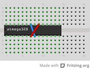
For a very quick setup all I do is connect VCC & AVCC to a power supply (3.3V or 5V) and the 2 GND pins to Ground. That’s it. It’s enough to get the chip going as long as it’s setup to use the internal oscillator.

basic_arduino_bb

If the chip arrives with a Uno Bootloader installed or even basic factory settings I prefer to change the settings to suit my needs. For this the fuses need to be set appropriately. The best resource I’ve found to determine the fuses is this link.

My preferred setup is to run the chip at 8MHz using it’s internal oscillator, no bootloader and brown-out detection at 2.7V. This gives me a setting of:

low_fuses = 0xE2
high_fuses = 0xDF
extended_fuses = 0x05

With this information I created my own Arduino board setting that I save in boards.txt under Arduino/hardware/breadboard/ folder.

atmega328abb.name=ATmega328 @ 8MHz – no bootloader

atmega328abb.upload.protocol=stk500
atmega328abb.upload.maximum_size=32256
atmega328abb.upload.speed=57600

atmega328abb.bootloader.low_fuses=0xE2
atmega328abb.bootloader.high_fuses=0xDF
atmega328abb.bootloader.extended_fuses=0x05
atmega328abb.bootloader.path=empty
atmega328abb.bootloader.file=empty
atmega328abb.bootloader.unlock_bits=0x3F
atmega328abb.bootloader.lock_bits=0x0F

atmega328abb.build.mcu=atmega328p
atmega328abb.build.f_cpu=8000000L
atmega328abb.build.core=arduino:arduino
atmega328abb.build.variant=arduino:standard

With this in place when I restart Arduino, I can see an additional entry under Boards.

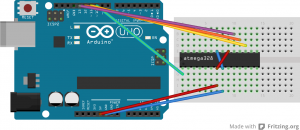
To burn the fuses to the chip I first load the ArduinoISP sketch on to an Uno (remember to choose Board = Arduino Uno when loading the ArduinoISP sketch). Then I hookup Uno pin 10 to Reset (PC6) on the chip, pin 11 to pin 11 (PB3/MOSI), pin 12 to pin 12 (PB4/MISO) and pin 13 to pin 13 (PB5/SCK). Note – 10, 11, 12 & 13 pins are used to allow communication via the SPI protocol.

arduino_programmer

Then I choose the Board (ATmega328 @ 8MHz – no bootloader) and then: Tools -> Burn Bootloader helps set the fuses. Note: Since the boot loader.file is specified as empty, the Arduino IDE will display an error. This is OK and the fuses have been reset.

If the chip came with an Arduino UNO bootloader it probably means the fuses are configured to expect an external 16MHz oscillator. In this case we need to add a crystal between XTAL1 & XTAL2 with 22pf bypass capacitors grounding both XTAL1 & XTAL2 pins. This is needed so that the chip can start up to receive the fuse set commands. Once the fuses have been set to use the internal oscillator, the crystal is no longer required.

To test everything went well, load up the blink sketch and upload it to the chip via “Upload Using Programmer”. Hopefully everything uploaded successfully and to see it in action hookup an LED to pin 13 via an appropriate resistor.

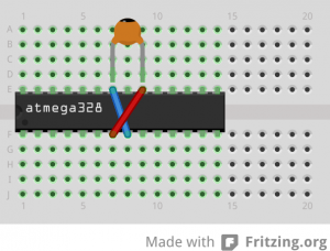
Finally when using the chip in a circuit I take the precaution to add a 0.1 uF bypass capacitor between VCC and GND. I also make sure I have a reservoir capacitor (say 47 uF) at the power supply to ensure a steady voltage.

basic_arduino_with_cap_bb

With just this setup I’ve been able to make very good use of these chips and have them run very reliably.